Circuit Board Pattern
Circuit Board Pattern - Web circuit board patterns play a crucial role in electronic design and pcb layout. How to make a printed circuit board (pcb) march 20, 2018 by suraj gehlot. Web a circuit board pattern refers to the visual representation of a circuit’s layout and design. Designing a professional circuit board pattern involves several steps, each requiring careful consideration and attention to detail. Web using pcb design layout guidelines can help engineers navigate potential problems that can arise during circuit board layout. This article is part of a series: These parts include resistors, switches, nodes, diodes, and more. This article explores the core principles of pcb layout, component placement, trace routing, signal integrity, and more. Pcb schematic and board layout how to generate manufacturing files for custom printed circuit boards; Web designing a professional circuit board pattern. Make your own printed circuit board at home to reduce problems that arise from loose connections on a breadboard. This article is part of a series: Pcb schematic and board layout how to generate manufacturing files for custom printed circuit boards; Free for commercial use high quality images 100,000+ vectors, stock photos & psd files. It consists of intricate configurations of lines, pads, vias, and geometric shapes that map out the arrangement of components and electrical connections on. These parts include resistors, switches, nodes, diodes, and more. Web circuit board patterns play a crucial role in electronic design and pcb layout. 100,000+ vectors, stock photos & psd files. Less searching, more finding with getty images. Free for commercial use high quality images. Web to design a printed circuit board (pcb), you need to draw holes, pads, and wires for your circuit. Web a printed circuit board (pcb) layout is the blueprint that guides the production of circuit boards which are the backbone of any electronic device. Pcb schematic and board layout how to generate manufacturing. Web circuit board patterns are like a roadmap for the circuit, containing a group of symbols representing parts of the circuit. Free for commercial use high quality images. These parts include resistors, switches, nodes, diodes, and more. Web explore authentic circuit board pattern stock photos & images for your project or campaign. Web using pcb design layout guidelines can help. Web circuit board patterns play a crucial role in electronic design and pcb layout. Free for commercial use high quality images. Web explore authentic circuit board pattern stock photos & images for your project or campaign. They define the interconnections, signal routing, and power distribution within the board, ensuring reliable signal transmission, minimizing interference, and optimizing system performance. Web a. Web a printed circuit board (pcb) layout is the blueprint that guides the production of circuit boards which are the backbone of any electronic device. Web a circuit board pattern refers to the visual representation of a circuit’s layout and design. Web circuit board pattern photos & images. Web circuit board patterns are like a roadmap for the circuit, containing. Web designing a professional circuit board pattern. Web this article examines essential factors regarding circuit board patterns in pcbs such as the types of patterns, advantages, how to choose pattern fabric. This article is part of a series: 100,000+ vectors, stock photos & psd files. Make your own printed circuit board at home to reduce problems that arise from loose. These patterns consist of copper traces that link multiple features, including resistors , integrated circuits, and capacitors , forming the complete course. Free for commercial use high quality images Less searching, more finding with getty images. Web explore authentic circuit board pattern stock photos & images for your project or campaign. Web find & download free graphic resources for circuit. Web explore authentic circuit board pattern stock photos & images for your project or campaign. How to make a printed circuit board (pcb) march 20, 2018 by suraj gehlot. This article explores the core principles of pcb layout, component placement, trace routing, signal integrity, and more. Web pcbs patterns are arrangements of electronic components and conductive pathways on a circuit. Web explore authentic circuit board pattern stock photos & images for your project or campaign. Web circuit board patterns play a crucial role in electronic design and pcb layout. Designing a professional circuit board pattern involves several steps, each requiring careful consideration and attention to detail. Free for commercial use high quality images Less searching, more finding with getty images. Web using pcb design layout guidelines can help engineers navigate potential problems that can arise during circuit board layout. Web a circuit board pattern refers to the visual representation of a circuit’s layout and design. Web pcbs patterns are arrangements of electronic components and conductive pathways on a circuit board. Web a printed circuit board (pcb) layout is the blueprint. This article is part of a series: Web circuit board patterns play a crucial role in electronic design and pcb layout. Web pcbs patterns are arrangements of electronic components and conductive pathways on a circuit board. These patterns consist of copper traces that link multiple features, including resistors , integrated circuits, and capacitors , forming the complete course. Web this. Web find & download free graphic resources for circuit board pattern. Web circuit board pattern photos & images. 100,000+ vectors, stock photos & psd files. Designing a professional circuit board pattern involves several steps, each requiring careful consideration and attention to detail. 100,000+ vectors, stock photos & psd files. These parts include resistors, switches, nodes, diodes, and more. Web explore authentic circuit board pattern stock photos & images for your project or campaign. Web find & download the most popular circuit board patterns vectors on freepik free for commercial use high quality images made for creative projects. Web to design a printed circuit board (pcb), you need to draw holes, pads, and wires for your circuit. Free for commercial use high quality images. These patterns consist of copper traces that link multiple features, including resistors , integrated circuits, and capacitors , forming the complete course. Web find & download free graphic resources for circuit board patterns. Web guide to ordering and assembling printed circuit boards. Pcb schematic and board layout how to generate manufacturing files for custom printed circuit boards; Web a printed circuit board (pcb) layout is the blueprint that guides the production of circuit boards which are the backbone of any electronic device. They define the interconnections, signal routing, and power distribution within the board, ensuring reliable signal transmission, minimizing interference, and optimizing system performance.
Circuit board seamless pattern background of Vector Image

Computer circuit board Seamless pattern Royalty Free Vector
How to design a professional and beautiful Circuit Board Pattern
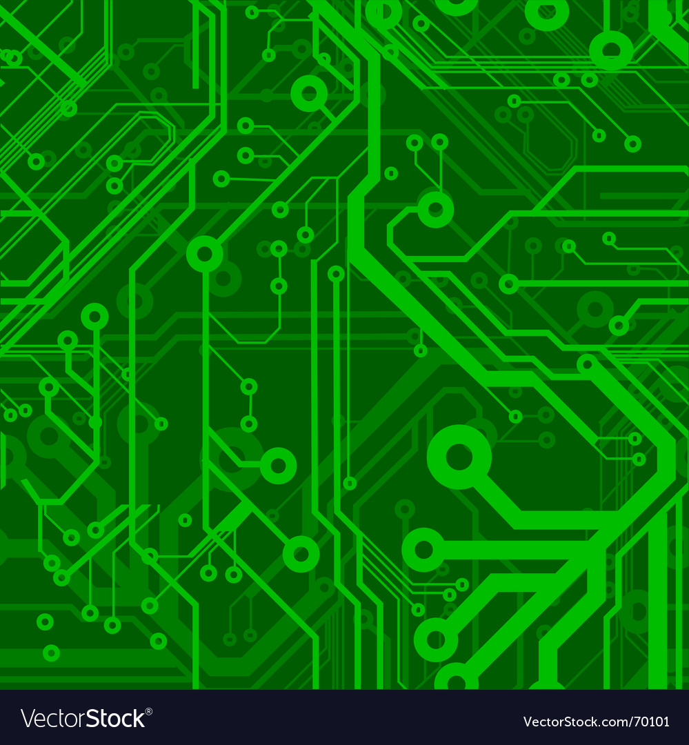
Circuit board pattern Royalty Free Vector Image
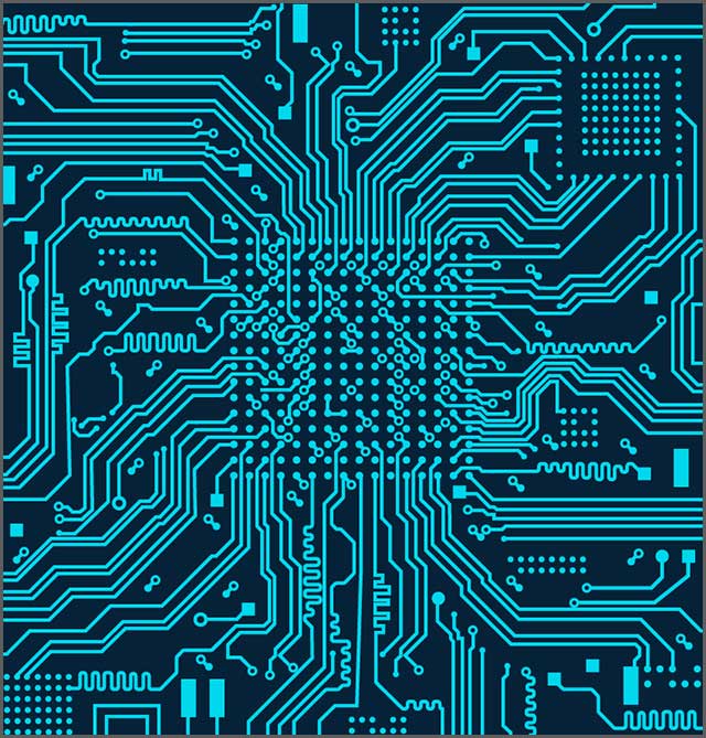
Circuit Board Pattern
How to design a professional and beautiful Circuit Board Pattern
Circuit Board 25 Pattern

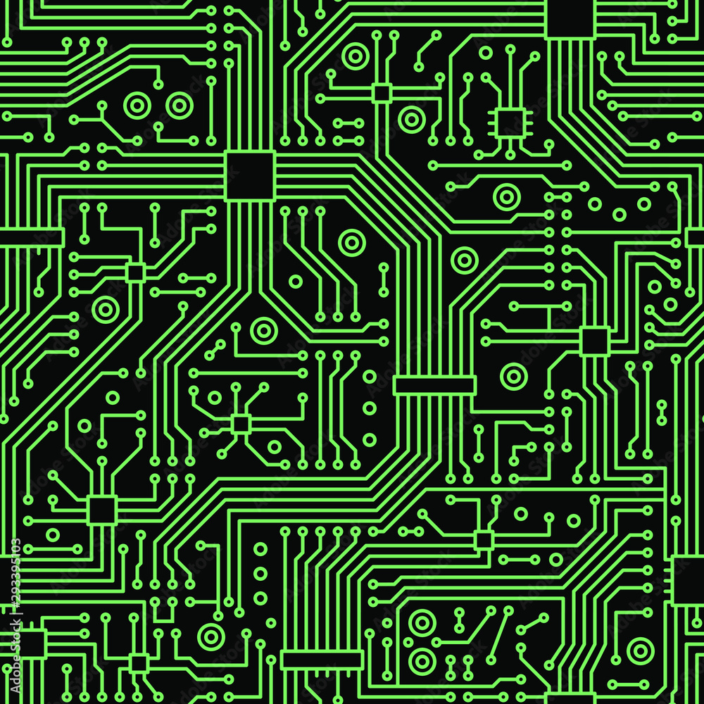
Green electronic circuit board pattern Free backgrounds and textures

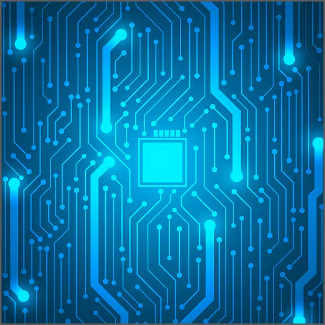
Circuit Board Pattern HighRes Vector Graphic Getty Images

Printed Circuit Board Vector Illustration 344822 Vector Art at Vecteezy
This Article Explores The Core Principles Of Pcb Layout, Component Placement, Trace Routing, Signal Integrity, And More.
Less Searching, More Finding With Getty Images.
Make Your Own Printed Circuit Board At Home To Reduce Problems That Arise From Loose Connections On A Breadboard.
The First Step In Designing A Circuit Board Is To Create A Schematic Diagram.
Related Post: